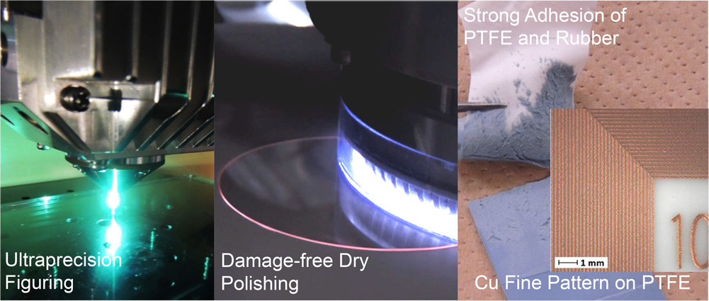
01Plasma nano-Manufacturing Process
Surface fabrication is based on the atmospheric-pressure plasma process that consists of the following three Fs:
Figuring(Shape Fabrication)
Plasma chemical vaporization machining (CVM)
Reactive plasma, which is locally generated under an open-air condition, is numerically controlled; therefore, shape creation and thickness distribution can be controlled with nanometer precision during dry etching for shape creation and removal of the work-affected layer.
Finishing(Surface finish)
Plasma-assisted Polishing
This is a dry polishing process that combines surface modification using plasma irradiation and removal of the modified layer by polishing with soft abrasive grains. Wide-gap semiconductor substrates, such as SiC, GaN, diamond, and various fine ceramics can be polished without causing any damage.
Functionalization (Surface Functionalization)
Heat-assisted atmospheric pressure plasma treatment
By performing plasma irradiation and surface heating simultaneously, the adhesion of each type of resin can be enhanced significantly. High adhesion, which is difficult to obtain using conventional plasma treatment, is provided to fluororesin. Fluororesin can strongly adhere to butyl rubber, silver salt ink, copper paste, PDMS, and other substances without an added adhesive.
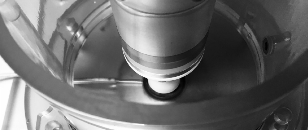
02Electrochemical nano-Manufacturing Process
Surfaces of hard, brittle, and difficult-to-machine conductive materials such as SiC can be softened by anodization, and the modified layer is removed without causing any damage by polishing with soft and fixed abrasive grains. Our goal is the actualization of high efficiency and low-cost slurry-less polishing.
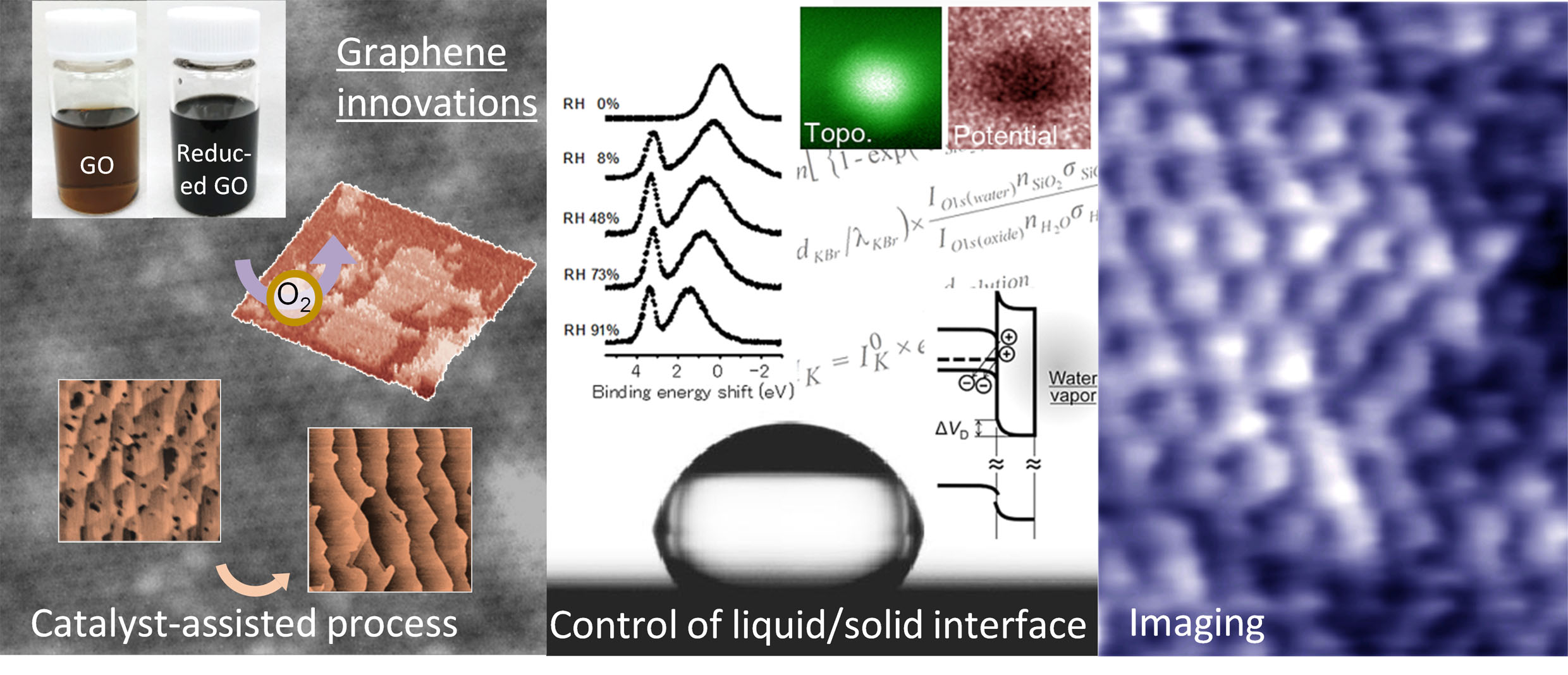
03Science of practical semiconductor surface
In our laboratory, we make full use of probe microscopic technology and surface-sensitive spectroscopic techniques, which can be used to evaluate the performance of surface creation processes for various materials, mainly semiconductors, at the sub-nanometer scale. The target processes include ultra-precise machining, cleaning, film formation and synthesis. In this manner, the above processes are comprehended with an extreme accuracy, or at the atomic, molecular and electron level, for further upgrading. In addition, by deepening the understanding of science on such practical surfaces, we challenge to develop novel processes to form well-controlled surfaces and to obtain nanomaterials. These procedures open the world of new nano-manufacturing science.
■Development of new catalyst-assisted nano-surface processes for semiconductors
■Molecular-level measurements of wetting properties on solid surfaces and their applications
■Observation of atomic structures of practical semiconductor surfaces after industrial processes
