Dedicated Equipment
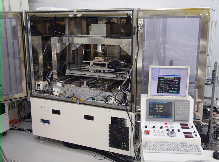
Numerically Controlled Plasma CVM Apparatus
Plasma etching apparatus utilizing locally generated atmospheric-pressure plasma. Numerical control of the work table allows for figuring shapes with nanometer order precision.
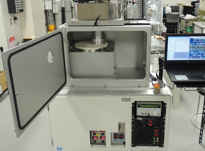
Plasma-assisted Polishing Apparatus
Through surface modification by plasma irradiation and removal of the modified layer by soft abrasive grains, 3-inch SiC, GaN, and sapphire wafers can be dry polished with high efficiency and without any damage.
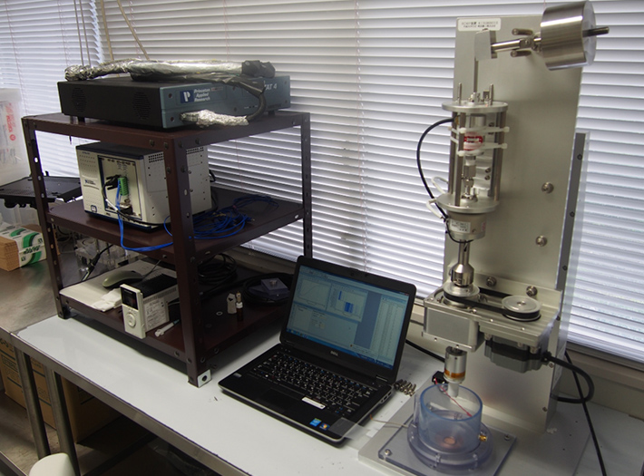
Electrochemical Mechanical Polishing Apparatus
This is an apparatus that examines fundamental electrochemical-mechanical polished characteristics of conductive hard and brittle substrates. The potential of the substrate with respect to the electrolytic solution is controlled by a potentiostat with three electrodes.
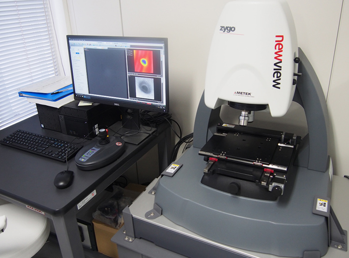
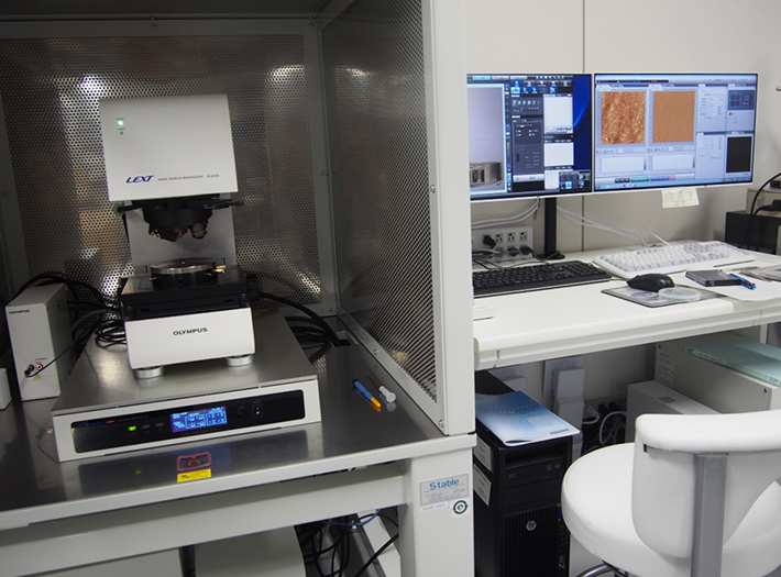
Scanning White Light Interferometer
This is a non-contact three-dimensional optical surface profiler using microscopic interference. The surface roughness of the substrate can be measured with sub-angstrom reproducibility.
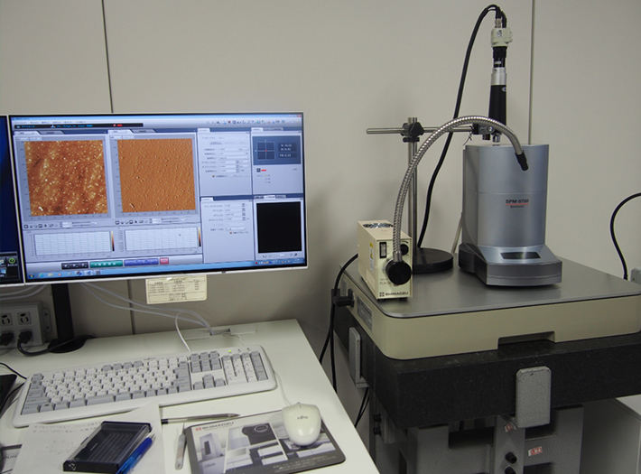
Atomic Force Microscope
This is a scanning probe microscope that can observe surface structures at the atomic level.
Nano Search Microscope
Optical microscopes, scanning laser microscopes, and scanning probe microscopes are integrated into an integrated microscope. The same point on observation targets can be seamlessly observed in the scale ranging from millimeters to nanometers, depending on the microscopic imaging technique used.
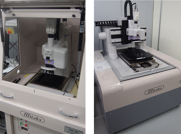
Laser Probe 3D Measuring Instrument
It is a non-contact three-dimensional shape measuring device consisting of a laser autofocus microscope for height measurement and high-precision XYZ stage, and there are two models: a high-precision type with Z resolution of 1 nm and a large-sample type with Z resolution of 10 nm.
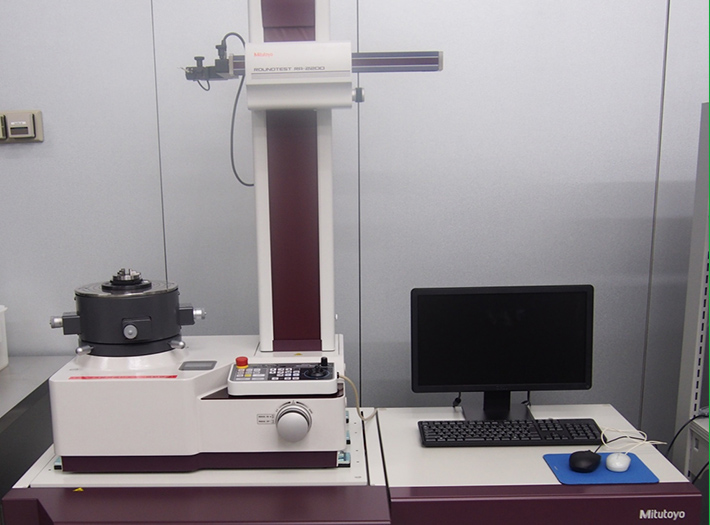
Roundness/Cylindricity Measuring Machine
s is a measuring device that measures the roundness of cylinders.
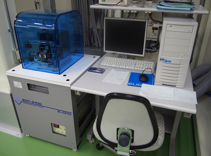
Nanoindenter
This is a measuring device that measures hardness and Young’s modulus of polar surface layers of samples, films, and polymers.
Noncontact Atomic Force Microscope
This is a scanning probe microscope that can observe surface structures at the atomic level. The probe tip does not touch the sample surface. Unlike familiar STM, non-conductive sample surfaces can be imaged.
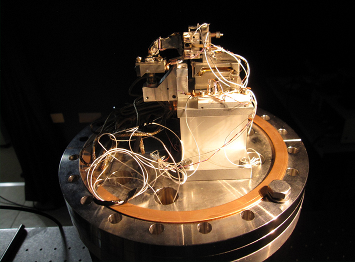
Electrical characteristics measurement setup equipping with surface preparation chambers
Under high vacuum conditions, the amount of gas molecules adsorbed onto a semiconductor surface can be controlled at the monolayer level. In addition, by fabricating an electronic device on the semiconductor surface, the impact of adsorbed gas molecules on the electrical characteristics of the device can be evaluated in situ.
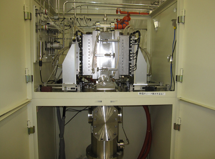
Thermal Oxidation Furnace
With an infrared light source, this setup thermally treats semiconductor wafers under high-purity oxygen gas conditions. With this apparatus, high-quality oxide films of nanometer level thickness can be formed uniformly across the wafer.
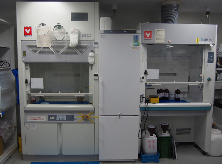
Fume hood
Local ventilation device that protect users from inhaling hazardous/toxic fumes and vapors in the use of chemicals.
Shared Equipment
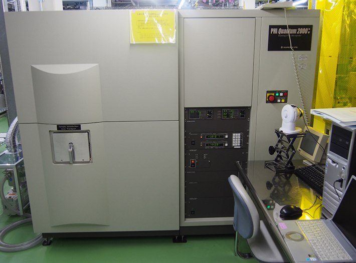
X-ray Photoelectron Spectroscopy
Sample surfaces are irradiated by X-ray, and by measuring the kinetic energy of photoelectrons released from the sample surface, this device analyzes the composition and chemical bonds of elements that constitute the sample surface.
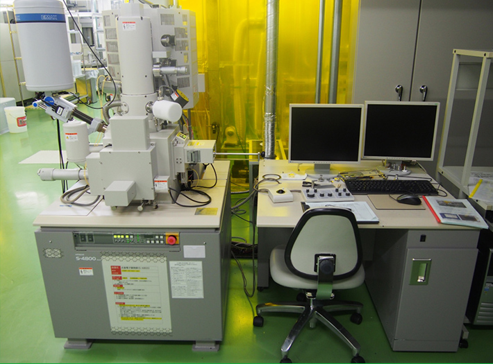
Scanning Electron Microscope
The surface structure of samples can be observed using a high-resolution scanning electron microscope equipped with a field-emission type electron gun. Since an energy dispersive X-ray spectrometry (EDX) device is attached, elemental mapping of samples is possible.
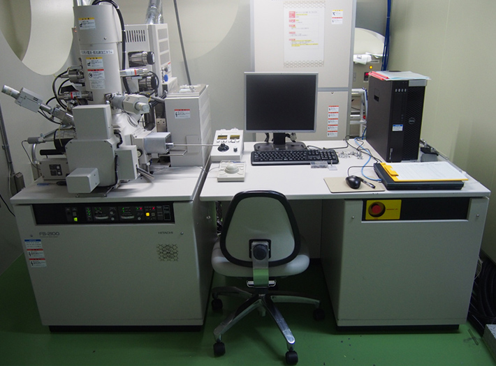
Focused Ion Beam System
This is a device that irradiates samples with a focused ion beam to prepare samples for observation of microfabrication and cross-section TEM (XTEM).
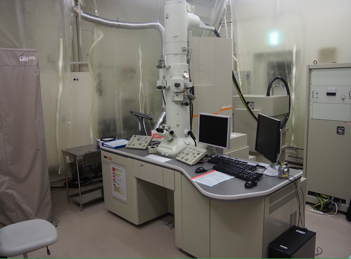
Transmission Electron Microscope
By irradiating the samples with accelerated and focused electron beams, structures can be observed in the enlarged projection of transmitted electrons, and crystalline structures can be analyzed through electron diffraction.
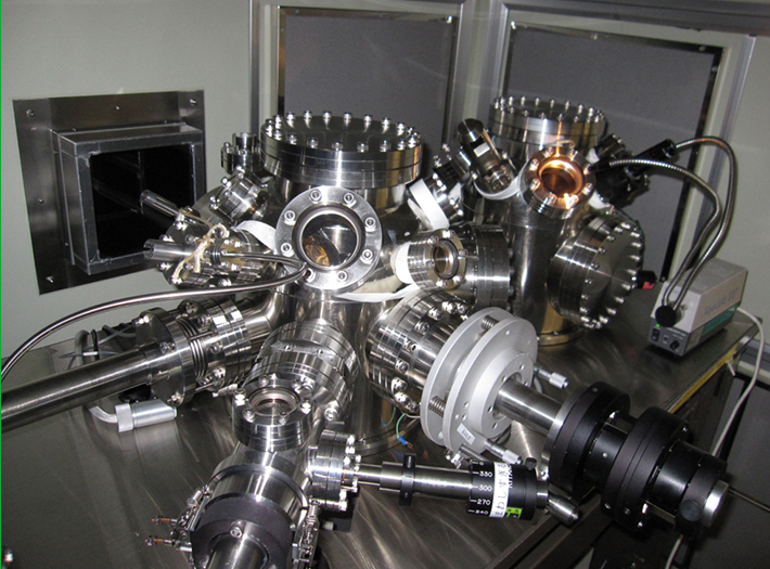
Scanning Tunneling Microscope
This is an ultra-high vacuum scanning tunneling microscope. Installed in a “clean room,” it is used to examine the atomic arrangement of semiconductor surfaces that have been obtained through etching and wet cleaning processes.
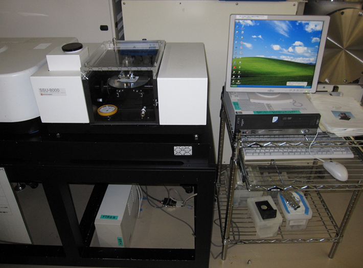
Fourier Transform Infrared Spectroscopy
By measuring the absorption spectrum of infrared rays, chemical bonds of samples can be analyzed. With a unique prism, the condition of the outermost layer of samples (contamination, oxide layer, and micro-roughness) is detected with high sensitivity.
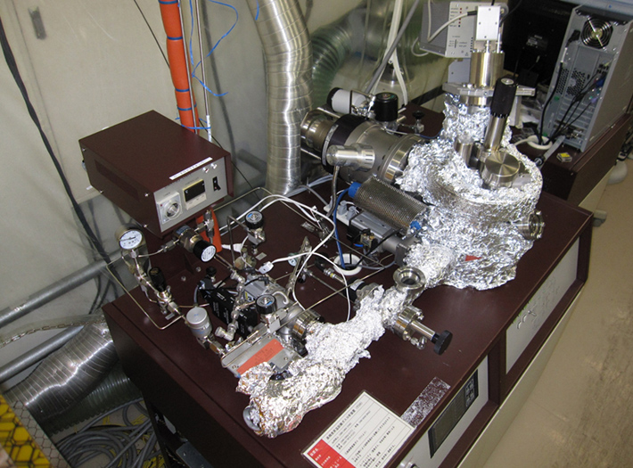
Thermal Desorption Spectrometry
Samples are heated in ultra-high vacuum, and the atoms or molecules released in vacuum are ionized. By determining the mass number and the density of the generated ions, absorbed species and bond strength on the sample surface can be evaluated.
