
MEMBER
Kazuya YAMAMURA
With a motto of “challenging the common sense,” which was the way my former teacher lived his life, I am developing new physiochemical processes with passion. As those who know me will tell you, I am an impatient person and once I’m develop an interest in something, I become “extreme” in my pursuit of the endeavor.
 Other Members
 Details
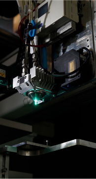
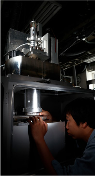
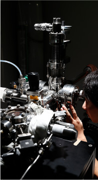
GALLERY
ACCESS
M1 Building, Room #426,#427
Department of Precision Engineering,
Graduate School of Engineering, Osaka University,
2-1 Yamadaoka,Suita, Osaka 565-0871 Japan
Phone: +81-6-6879-7294
Details
Contact