Figuring with nanometer precision
by Plasma CVM
(Chemical Vaporization Machining)
Increased etching rate through the application of atmospheric-pressure plasma
Damage free because of the removal by chemical vaporization
There is no erosion of electrodes and reproducibility and stability are good
Since it is a non-contact process, there is no impact from vibration or thermal deformation → removes copy principle
Si, SiO2, SiC, Si3N4, and diamond, among others, can be etched
Schematic of Plasma CVM

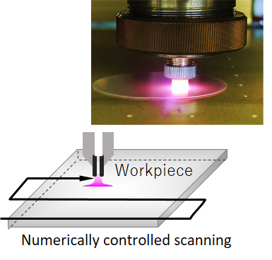
<Process flow of Numerically Controlled Plasma CVM (NC-PCVM) >
step1Shape measuring
step2Simulation
step3Shape correction
step4Shape accuracy wit nanometer order

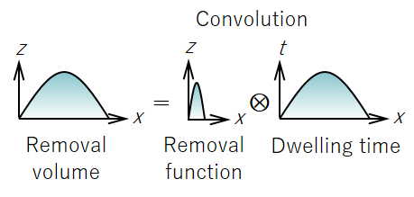
Based on the numerically controlled scanning of localized plasma, the shape is modified and the target shape can be obtained deterministically with nano-precision without using a trial and error approach.
Thickness distribution correction of quartz crystal wafer

