- HOME
- ABOUT
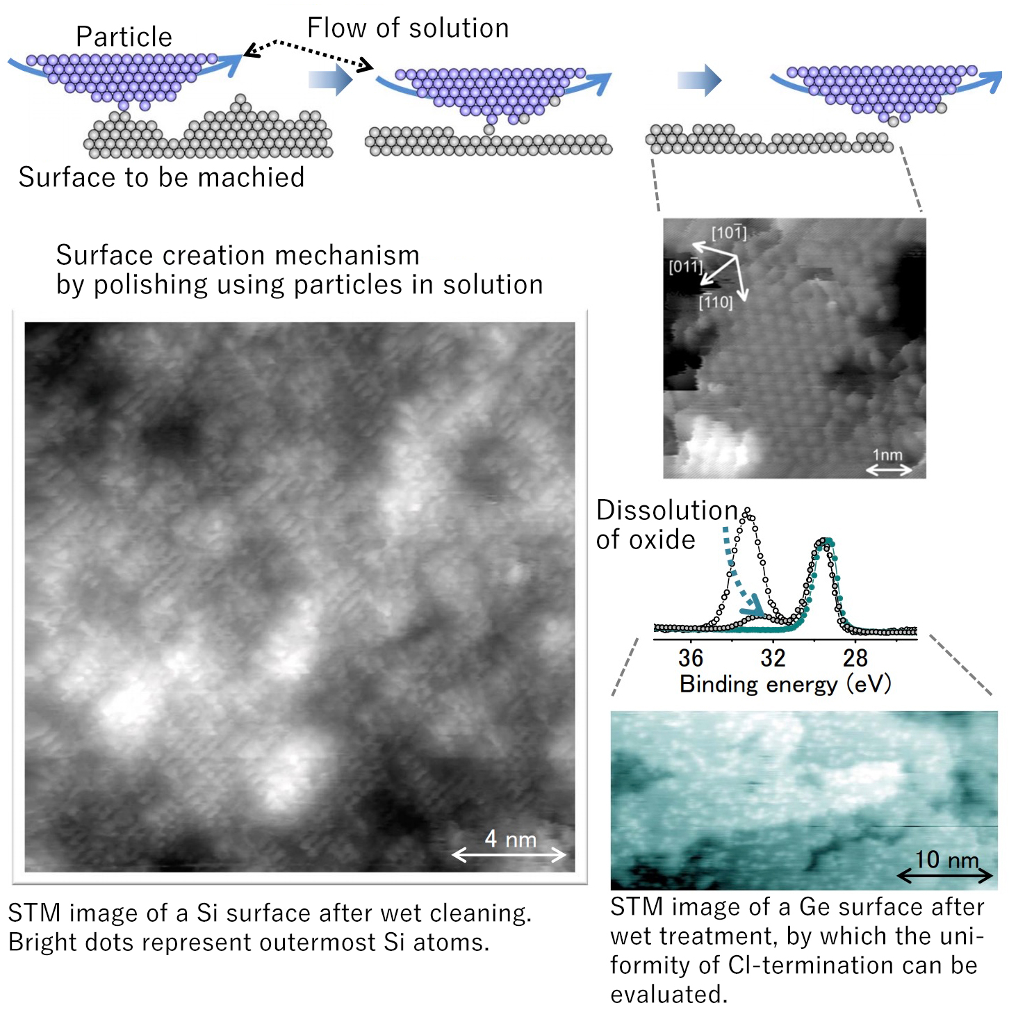
- Observation of atomic structures of practical semiconductor surfaces after industrial processes
Observation of atomic structures of practical semiconductor surfaces after industrial processes
By combining ultraclean technology and scanning tunneling microscopy observations, we can visualize the atomic arrangement of practical semiconductor surfaces to understand:
・Wet cleaning characteristics
・Ultra-precision machining characteristics
・Passivation properties of surface dangling bonds